")
There are two main materials for quartz wafers: fused silica quartz and single erystal quartz.
Fused silica is vitreous quartz, so it is isotropic. Fused silica is hard and has a very low coefficient of thermal expansion. There are many types of fused silica, each with different uses. We introduce three kinds here: JGS1, JGS2, JGS3. .
● JGS1, has good transparency in the ultraviolet and visible wavelength bands, does not contain bubbles and impurities, the materials used in the field of high-energy lasers, can be used to make optical components: lenses, prisms, etc.
● JGS2 is usually used for mirror substrates and contains many small bubbles.
.● JGS3 has good transmittance in the infrared band, but contains a lot of bubbles.
All single crystal quartz is grown from a special seed crystal. The different cutting types will result in different positioning of the seed crystal. -One type of seed crystal is inside the wafer, named "Wi thSeed", and the other type of seed crystal is not inside the wafer, so it is named "Seedless". Single crystal quartz can be divided into three zones: X/Y and Z zones. Seedless means that the wafer is in a pure X/Y or Z zone.
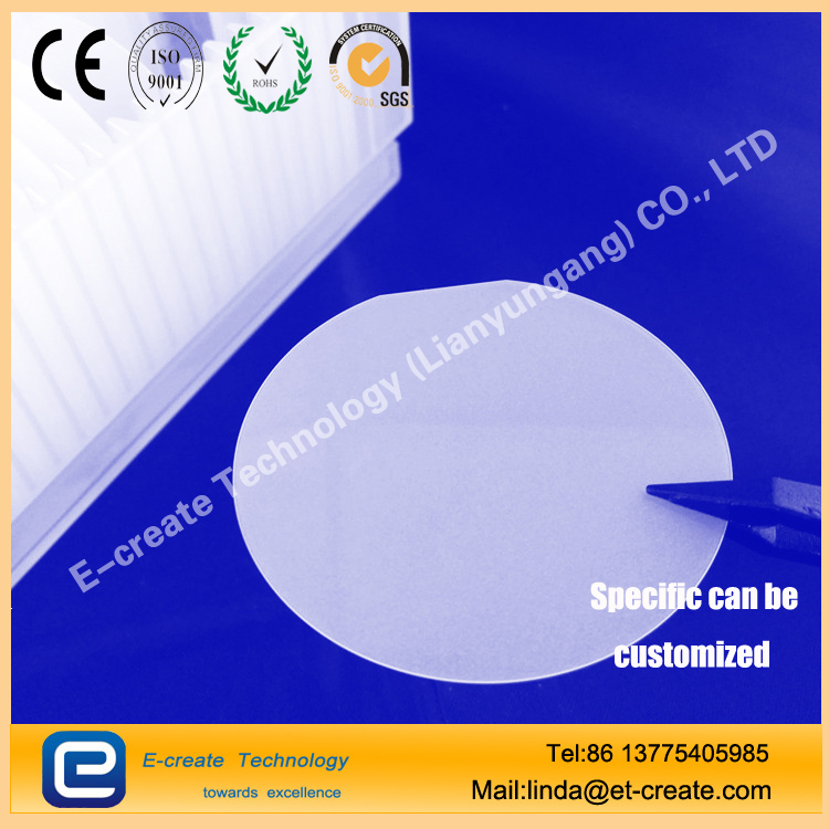
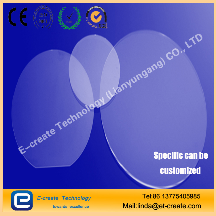
Quartz wafer is the most widely used optical material. Due to its high purity, low thermal expansion coefficient, high tensile strength, high optical transmission and unique electrical properties, quartz wafers are widely used in PLC planar waveguide splitter chips , MEMS, high-tech semiconductors, etc. Our company has long-term production of high-precision quartz wafers with thickness ≧0.1mm and dimensions ≧Φ2". In addition to the conventional Φ4”, Φ5”, Φ6”, Φ8”, Φ12", other sizes can be customized. Quartz wafers are usually made of Corning, Nikon, Heraeus and other materials. If you need to customize quartz wafers of other materials, please contact our sales staff.
规格 | 4 inch | 5 inch | 6 inch | 8 inch | 12 inch |
直径 | 100 ± 0.1 mm | 125 ± 0.1 mm | 150 ± 0.1 mm | 200 ± 0.1 mm | 300± 0.1 mm |
厚度 | 500 ± 5 um
或定制 | 625 ± 5 um
或定制 | 675 ± 5 um
或定制 | 725 ± 5 um
或定制 | 900± 5 um
或定制 |
粗糙度 | Ra ≤ 1 nm | Ra ≤ 1 nm | Ra ≤ 1 nm | Ra ≤ 1 nm | Ra ≤ 1 nm |
翘曲度 | ≤ 10um | ≤ 10um | ≤ 10um | ≤ 10um | ≤ 10um |
平整度 | ≤ 3 um | ≤ 3 um | ≤ 3 um | ≤ 3 um | ≤ 3 um |
表面质量 | 20/10 | 20/10 | 20/10 | 20/10 | 20/10 |
形状 | 圆形, 带定位边, 带定位角 |
倒边 | 45°, SEMI Spec; C Shape |
材质 | Corning, Nikon, Heraeus etc. |
备注 | 石英晶圆可定制 |


")