")
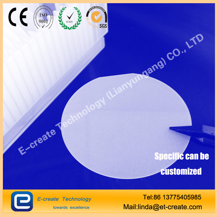
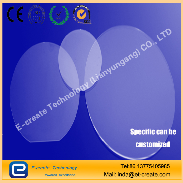
We can provide customers with high-precision glass wafers with thickness ≧0.1mm and dimensions ≧Φ2", which are used in CMOS, CCD sensors, integrated circuits or micromechanical component packaging (MEMS), communication and data processing, High-tech products such as optics, electronic products, home appliances, military industry, scientific research, etc.
Glass wafer plus technical parameters:
a) Material: Corning E-XG, PYREX7740, quartz glass, BOROFLOAT, B270, D263T, AF32, BK-7
b) Standard thickness: 0.1mm, 0.145mm, 0.2mm, 0.3mm, 0.4mm, 0.5mm, 0.7mm, 1.0mm, 1.1mm, 1.5mm (thickness tolerance ±0.02mm)
c) Standard size: Φ2", Φ3", Φ4", Φ5", Φ6", Φ8", Φ12" (other sizes can be customized)
d) Appearance: 60/40; 40/20; 20/10
e) Surface roughness (Ra)<1.5nm
f) Parallelism <0.01mm
Basic properties of Corning E-XG glass wafers:
技术参数: |
Density/密度(g/cc) | 2.3 |
Thermal Expansion/膨胀系数 | 3.0 |
Transmittance/透光率 | >90% |
softening point/软化点 | 971℃ |
TTV/平整度 | <0.005 |
Bow/翘曲度 | <0.01 |
Warp/弯曲度 | <0.01 |
Vickers Modulus/维氏硬度 | 640 |
Features:
●Special glass material application
●Experience in polishing field, unique surface quality
●Can be used in clean rooms for packaging ready-to-use substrates
●Structural wafers with excellent tolerances
●Customer-specified products that meet all requirements and industrial standards (such as SEMI)
●Integrated production steps that meet all requirements of ISO 9001:2000
typical application:
●Micro optics
● MEMS (pressure sensor, accelerometer...)
● Wafer-level packaging (image sensor packaging...)
●Bioengineering (microfluidics, DNA analysis...)
●And many other customer specified applications
g) Each edge is blunt C0.05~0.2mm
h) Crack <0.2mm, no internal crack
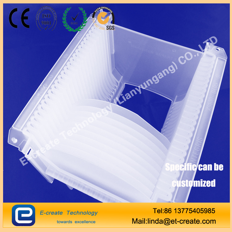
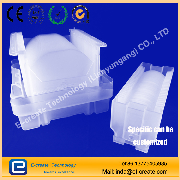
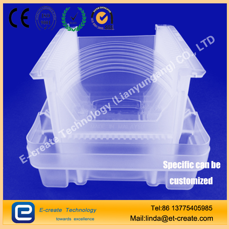
i) The surface is clean, free of marks and stains, packed in ultra-clean bags or single-piece boxes.


")
")
")